Overview
SERENITY is a carrier card for the phase-2 upgrade of the CMS experiment
at the LHC at CERN. It has been designed in a way which means it can be used in different capacities across
many sub-detectors. It is primarily a data engine allowing high data throughput (up to 5TBps per carrier board), utilising
either electrical or optical SAMTEC Firefly connectors and coupled with a flexible firmware stack (EMP) which allows
rapid algorithm development independent of the underlying infrastructure or even choice of FPGA.
More details about the technical specifications can be found under
short summary and getting started
documentation can be found under hardware setup guides.
Information for connections to initially program the FPGA daughter cards can be found here.
A technical paper describing the current status of SERENITY for CMS the phase-2 upgrade was presented at TWEPP’18:
SERENITY and associated components
SERENITY itself is a PCB carrier card with two daughter card sites (interposers X0/X1), a small CPU (COM Express mini)
a small service FPGA (artix) based around an ATCA form factor (power, ethernet, clock, cooling) with the possibility of
a micro-backplane adaptor for benchtop usage.
The SERENITY design takes advantage of a generic approach to the firm/software benefiting from the previous
EMP developments as part of the MP7 trigger board for the phase-1 CMS upgrade.
The following bullet points try to clarify the interconnectivity between the components:
Clock Distribution:
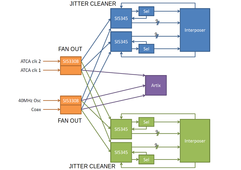
There are two reference clock inputs on the ATCA backplane (can also be applied on the SMA connectors on the micro-backplane adaptor) in addition there is an MMCX coax connector on
the carrier board (differential using two MMCXs) and an internal 40MHz crystal. Each of these four clocks can be distributed to the fan out and selected in the artix or at a
daughter card site. For the interposers there are two jitter correctors which then allow two reference clocks to be distributed to the FPGAs (multi-gigabit-transceivers). This then allows a choice
of reference clock depending upon the requirements - for example front-end board input would be phase locked to the LHC clock, whereas the output could be an asynchronous link.
A simpler way to consider the clock is that there are four input sources: 2xATCA, MMCX-coax, crystal and two inputs for each
transceiver (ref-clock-0 and ref-clock-1). The distribution is carried out by the global fan-out and then the local jitter correctors for each daughter card site. The control
of the clock selection is carried out by EMP control.
The LHC will provide two potential reference clocks: 40 MHz (LHC) and a higher frequency more precise 320 MHz (LHCP) cleaner one.
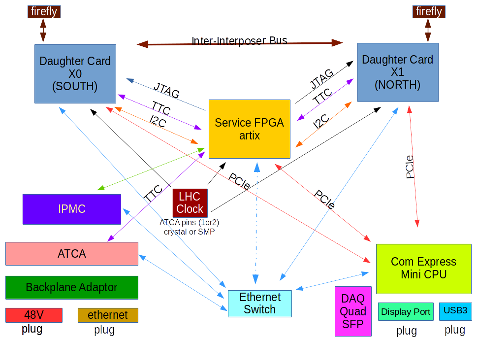
SERENITY Logical Connectivity
The SERENITY carrier card is designed around a flexible connectivity paradigm.
This means that there are a number of ways in which to communicate with the
carrier card and the attached daughter boards.
The following is a logical diagram derived from the board schematic
incorporating all the connection possibilities:
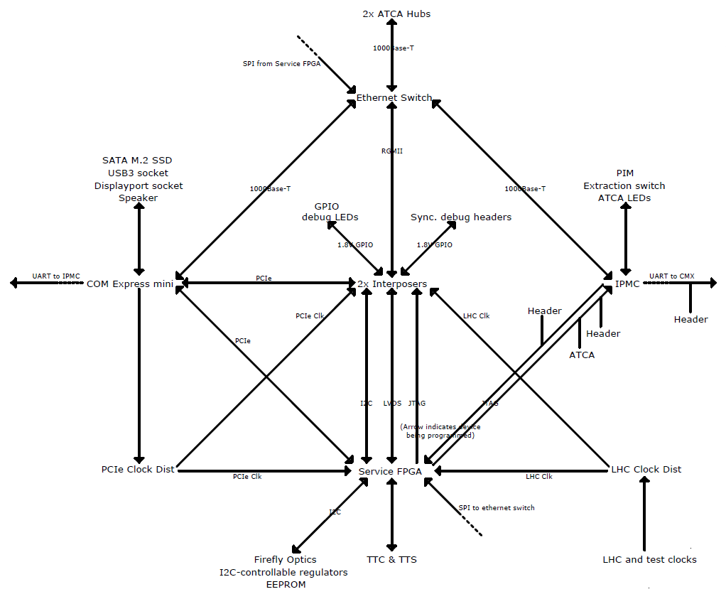
A version showing it as physically represented on the board can be at the bottom.
Connectivity: Use cases
The diagram above displays the complexity in the ways in which communication can be carried out.
Initially the recommended method of communication is:
Ethernet to the ComExpress CPU (through the ATCA backplane)
JTAG for direct programming of the FPGA Daughter Card sites
PCIe to “talk” to the daughter cards through the CPU (empbutler etc…)
The main in-use connetivity would be the following:
Slow Control Connectivity:
The connections for slow-control (configuration, temperature read-out, diagnostics, fan-control) and also ETHERNET communication
allows connection between the ATCA, IPMC and COMExpress. Optionally it could also communicate with the ARTIX (not foreseen).
A standard configuration method would involve communicating through the ATCA to the ETHERNET-switch and then routed to
the target of either the IPMC or the ComExpress:
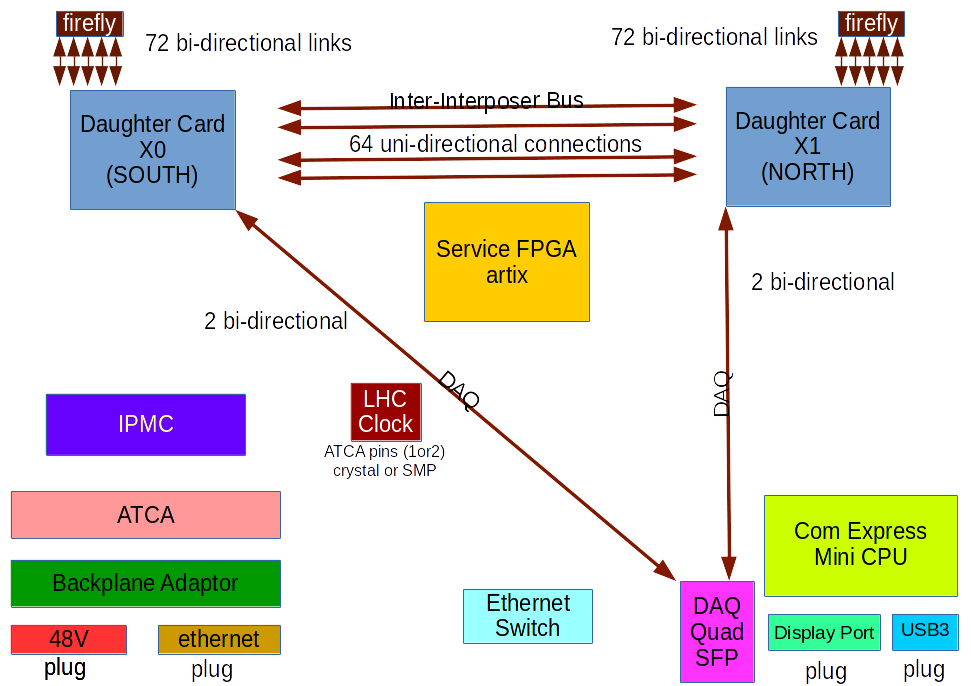
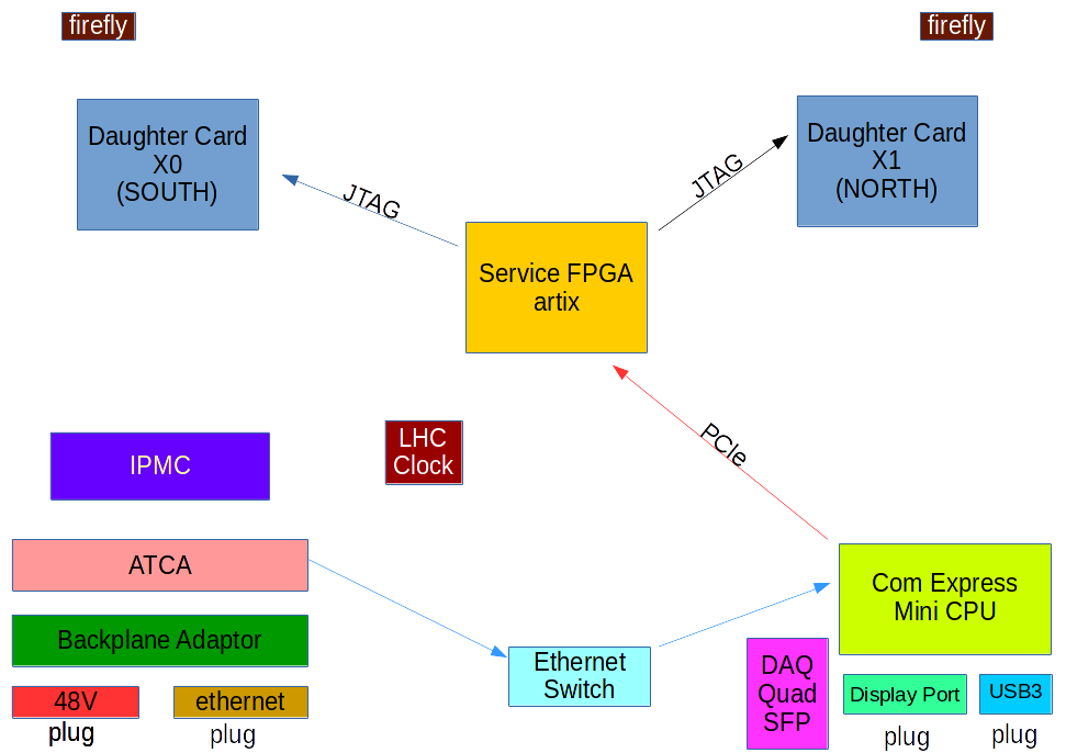
High Speed I/O:
The main IO of the board is carried out through the SAMTEC firefly transceivers (72-bi-directional optical/electrical connectors per
daughter card site. In addition there are 64 uni-directional lanes between the two daughter card sites. For DAQ purposes there
are a further 2 bi-directional links per interposer connected to a Quad SFP mounted next to the ComExpress at the rear (“east”) of
the board:
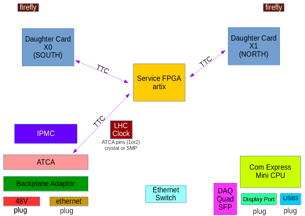
TTC (Trigger):
The TTC and TTS allow connectivity between the ATCA backplane and the interposers via the artix service FPGA:
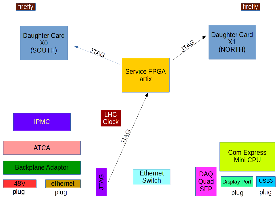
JTAG:
There are three main methods to program the FPGA daughter cards:
ATCA → ETHERNET-switch → ComExpress → PCIe → artix → JTAG →
daughter-card.
ComExpress → PCIe → artix → JTAG → daughter-card.
JTAG directly → artix → JTAG → daughter-card.
The first would be an external method, the second would be loading internall from e.g. an SSD and the third is the process
if connecting vivado directly to the carrier card.
For direct connection using Vivado the JTAG interface should be connected to the header marked “IPMC” on the SERENITY
carrier card. This routes the JTAG information through the artix FPGA to the chosen end-point (within Vivado).
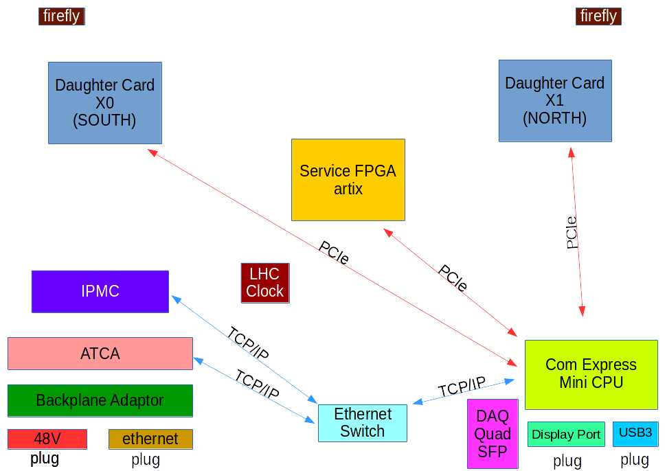
Logical-Diagram
As it is laid out on the board the connection options look like this:
edit this page